

Through-hole components remain common in power supplies, industrial controllers, and electronic products that use connectors or components requiring mechanical support. In high-volume production, soldering every lead manually can be inefficient and inconsistent. Wave soldering provides an automated alternative by forming multiple solder joints in a single pass.
During the process, a PCB travels over a controlled wave of molten solder. The solder wets exposed component leads and copper surfaces, then flows into plated through-holes to establish electrical connections and mechanical support.
How the Wave Soldering Process Works?
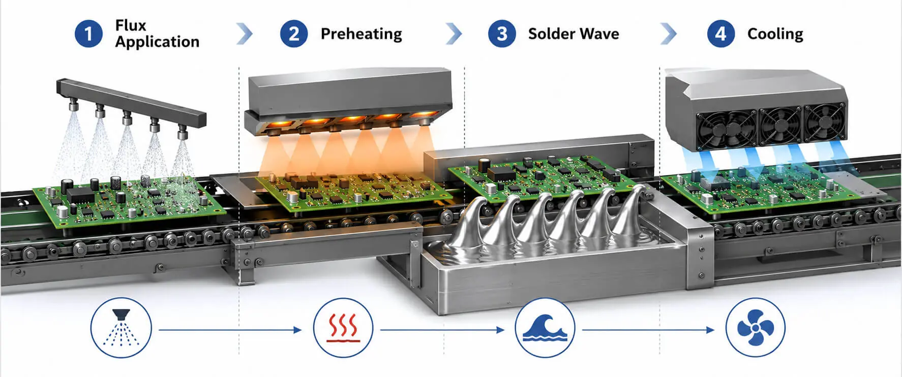
Wave soldering typically involves four stages: flux application, preheating, soldering, and cooling.
1. Flux Application
Flux is applied to the underside of the PCB, commonly using a spray system. Some older equipment uses foam fluxing, while selective fluxing can target specific areas on mixed-technology assemblies.
Flux removes surface oxides from pads, component leads, and plated through-holes while limiting further oxidation during soldering. It also promotes solder wetting. Too little flux can cause poor wetting or incomplete hole fill, while excessive application may leave unwanted residues or contribute to soldering defects.
2. Preheating
The PCB passes through preheating zones that use infrared heaters, convection heaters, or both. Preheating evaporates volatile flux solvents, activates the remaining flux chemistry, and reduces the thermal shock caused by contact with molten solder above 250°C.
It also helps equalize temperatures across the board. This is particularly important for multilayer PCBs and assemblies with large copper planes or components with high thermal mass.
3. Contact with the Solder Wave
A pump circulates molten solder from a temperature-controlled pot through specially designed nozzles to create a stable wave. The conveyor usually carries the PCB at an angle, exposing its underside to the solder while keeping the component side above the molten bath.
During contact, solder wets the exposed metal surfaces, and capillary action draws it into plated through-holes around component leads. As the board leaves the wave, surface tension helps remove excess solder and form joint fillets.
Two common configurations are used. Single-wave soldering uses one wave and is generally suitable for simpler through-hole layouts. Dual-wave soldering uses a turbulent first wave to improve solder penetration and hole filling, followed by a smoother wave that helps remove excess solder and reduce bridging, icicles, and uneven fillets. The choice depends on component spacing, board layout, and assembly complexity.
4. Cooling
After soldering, the assembly cools so the solder solidifies into permanent electrical and mechanical connections. Controlled cooling helps limit thermal stress in the PCB and its components. The board can then proceed to inspection and electrical testing.
Important Wave Soldering Parameters
The following values from the source article provide starting points, not universal settings for every assembly.
Solder pot temperature: 245–260°C for lead-free solder and 245–250°C for SnPb solder.
PCB topside preheat temperature: 90–130°C.
Conveyor speed: 0.8–1.8 m/min.
Solder contact time: 2–4 seconds.
Conveyor angle: 5°–7°.
Wave height: 50–70% of PCB thickness.
Flux application: Approximately 2–5% solids, depending on the flux type.
These parameters interact, so changing one may require adjustments to others.
For example, increasing conveyor speed reduces contact time and may lead to insufficient hole fill. Moving too slowly increases thermal exposure and can contribute to bridging, excessive solder deposits, or component damage. Similarly, increasing solder temperature is not always the correct response to poor wetting. Flux coverage, preheating, contact time, and board design should also be checked.
Wave height, immersion depth, and conveyor angle influence how the board contacts the solder and how excess solder drains away. The correct combination depends on the assembly and the equipment being used.
Thermal Profiling and Process Validation
Thermal profiling helps establish whether the board receives suitable preheat and solder exposure. Thermocouples are attached to representative pads, plated through-hole leads, or critical component locations, and the instrumented PCB is passed through the complete process.
The source article references IPC-TM-650 and IPC-7530 for guidance on thermocouple attachment and profile measurement. For robust lead-free processes, it gives a typical PCB topside temperature of 110–130°C before soldering. It also describes time above liquidus (TAL) as essentially the period of contact with the molten solder wave, which must remain within the required process window. The profile should confirm that the PCB cools below approximately 100°C before leaving the cooling section.
Recorded profiles help identify hot and cold spots so the process can be adjusted accordingly. This is more reliable than changing process settings based only on visual inspection of solder joints.
Choosing the Right Soldering Method
Single-wave soldering is generally appropriate for simple through-hole boards, where wave height, conveyor speed, and solder drainage are key controls. Dual-wave soldering is useful for denser through-hole or mixed-technology assemblies, but requires careful balancing of the turbulent and smooth waves.
Selective soldering is another option for complex boards with only limited through-hole areas. It uses a small programmable nozzle to solder selected joints, allowing more localized heat control. Its nozzle path and dwell time require attention, and the process is generally slower than wave soldering.
The most suitable method depends on the board layout, component mix, production volume, and soldering requirements.
Practical Manufacturing Considerations
Reliable solder joints depend on more than the solder pot temperature. Flux coverage, preheat, wave geometry, contact time, and cooling must be considered together. Boards with dense component spacing or mixed surface-mount and through-hole technology may require particular attention when selecting the process.
For suitable through-hole and mixed-technology assemblies, PCBCool provides PCB manufacturing and assembly services, with wave soldering or manual through-hole soldering selected according to the assembly